
PVD Conforms to Smaller Features
In planar magnetron systems, ions from an argon plasma dislodge atoms from the target surface. The target serves as the cathode, and magnets confine the emitted electrons near its surface. The magnets thus increase the ion density in the plasma, which in turn increases the number of sputtering collisions and the deposition rate. The sputtered atoms are essentially ballistic, so they will strike the substrate surface from all angles.
This method works very well for deposition onto flat surfaces. Unfortunately, real wafers have topography that becomes more severe as feature sizes shrink. Aspect ratios for contacts in the 0.18 mm generation are typically between 8 and 10. The shadows cast by such tall sidewalls reduce bottom coverage. Metal deposited on the tops of raised features tends to overhang, as a rising loaf of bread overhangs the edge of the pan (hence the term, "bread loafing"). In extreme cases, overhang from adjacent features can "pinch-off" deposition into a trench or contact hole altogether, creating a void.
Even as higher aspect ratios make conformal coverage more difficult, Cu metallization makes achieving it more important. Leaks in barrier layers allow Cu diffusion. Holes in Cu seed layers reduce electroplating efficiency. Equipment makers are investigating ways to keep the advantages of sputtering while improving step coverage in high aspect ratio features.
For example, today <%=company%> (San Jose, CA) announced a new system based on hollow cathode magnetron sputtering (HCM) (See "PVD System for 0.18 Micron Production"). This system relies on the same fundamental physics as planar magnetron sputtering to create the plasma. However, HCM uses a cup-shaped target and a high-density plasma to achieve greater than 90% ionization of the sputtered atoms as compared to less than 10% in a conventional planar system. Neutral atoms are trapped by the target and recycled into the plasma. Once the metal is ionized, magnets or bias current can steer it towards the substrate. Novellus claims to achieve on the order of 40% bottom coverage in a 0.25-mm, 5:1-aspect-ratio contact hole, as opposed to less than 5% coverage for planar sputtering.
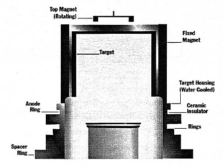
Schematic diagram of Novellus' hollow core magnetron system.
Applied Materials (Santa Clara, CA) claims to achieve similar results by placing an inductively coupled plasma between the target and the substrate. These systems ionize the sputtered atoms, which can then be steered to the substrate by an RF or DC bias.
Other alternatives to conventional planar magnetron sputtering include collimated sputtering and chemical vapor deposition (CVD). Collimated sputtering physically guides the sputtered items toward the substrate. Deposition on the collimator is a source of particles, though, and throughput declines. This method is not able to achieve sufficient bottom coverage at very high aspect ratios.
CVD is much less subject to step coverage problems, and is commonly used for Si and SiO2 layers. Most available precursors for metals are metal-organic compounds, however. Carbon and other organic constituents tend to degrade the film quality and electrical properties.
Once, the shortcomings of collimated sputtering were seen as an argument for metal CVD. Now, the latest evolution of PVD suggests that the old workhorse will not go quietly out to pasture.
By Katherine Derbyshire
Chemical vapor deposition (CVD): a deposition process in which a non-volatile film forms on the substrate due to the reaction of vapor phase precursors.
Physical vapor deposition (PVD): a deposition process in which the solid or liquid source material is converted to a vapor by mechanical or thermal means, transported to the substrate, and condensed from the vapor onto the substrate. Sputtering, which mechanically knocks the source atoms loose, is the most common PVD method in semiconductor manufacturing, and the two terms are often used interchangeably.
Sputtering: See physical vapor deposition.