
Vistec Semiconductor Reports Success In EUV Mask Registration Metrology

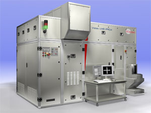 Weilburg, Germany - In cooperation with a Japanese EUV mask supplier, Vistec Semiconductor Systems demonstrated impressive measurement results on EUV masks by using the Vistec LMS IPRO4 registration metrology system.
During SPIE Advanced Lithography Conference in San Jose, California two weeks ago leading chip-makers made clear that EUV is an absolute must for IC production at 22 nm and beyond. Other viable options seem to be out of sight. According to reports from Solid State Technology, Ben Enyon, associated director of Sematech's lithography division in Albany, N.Y., stated that the technology will not be suited for volume production until an entire infrastructure is in place.
Metrology, and the extremely tight EUV mask to mask overlay in particular, is a key component for this infrastructure.
At the European Mask and Lithography Conference (EMLC) in Dresden, Germany Vistec recently published new registration metrology results on EUV masks using the state-of-the-art metrology system LMS IPRO4. Measurement repeatability on EUV masks proved to be better than 0.8 nm and accuracy was below 1.6 nm (3 sigma) over the entire active array of 100 x 128 mm.
"The performance achieved is considered to be perfectly suited to characterize sample R & D masks for EUV lithography," explained Klaus-Dieter Roeth, Vistec's Senior Product Manager for Mask Metrology.
The Vistec LMS IPRO4 was introduced in July 2007, and six leading-edge mask shops world-wide have already ordered systems; additional orders are expected soon. Apart from the extraordinary measurement capability on EUV masks, all installed LMS IPRO4 systems have demonstrated excellent performance exceeding all system specifications by at least 25 – 30 %. "We are very pleased with the metrology efficiency of the LMS IPRO4 that is deeply rooted in Vistec's many years of expert knowledge in system integration of mask metrology equipment and its future-oriented design. Our next generation tool, the Vistec LMS IPRO5, currently under development, will further enhance EUV-capabilities, and specifically address double patterning requirements. It will be launched next year." commented General Manager Gerhard Ruppik.
Vistec Semiconductor Systems GmbH:
Vistec Semiconductor Systems GmbH provides key technology used by all leading semiconductor manufacturers, and many research institutes around the world. Their innovative product portfolio includes inspection systems, defect detection and classification systems, and metrology systems for mask and wafer manufacturing. Their systems are used for microchip and photomask production as well as for scientific and commercial research. In addition to the production facility in Germany, the company also maintains support centers in the USA, Japan, China, Singapore, Taiwan and Korea.
Vistec Semiconductor Systems GmbH, Weilburg is part of the Vistec Semiconductor Systems Group which consists of three business units:
- Vistec Semiconductor Systems GmbH located in Weilburg, Germany
- Vistec Electron Beam GmbH located in Jena, Germany
- Vistec Lithography Inc. located in Watervliet, N.Y., USA
SOURCE: Vistec Semiconductor Systems