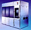
Step-and-Scan Lithography Systems

SVG Lithography 's Micrascan II+ and II+/QML (below .30 micron) and Micrascan III (below .25 micron) are based on technology that has been used in production at some of the world's most advanced fabs. Proven components were enhanced and combined with a low-distortion optics system to improve exposure field, overlay, throughput, and process latitude.
The step-and-scan products, which can be integrated with most photolithography processing systems, provide critical dimension control and low distortion across the wafer. Catadioptric projection optics mix refractive and reflective optics, making the subsystem more compact and less sensitive to changes in ambient temperature and pressure than refractive-only optics. The products' combination of scanning stages and catadioptric optical design has reduced lens distortion to < ±30 nm over the entire exposure field.
An on-the-fly wafer focus and leveling system continuously reads and corrects for changes in the Z-position of the wafer surface, and maintains the wafer in the optimum focal plane during exposure. Catadioptric design gives the optical system flat focus, long-term stability, and insensitivity to atmospheric variations, virtually eliminating internal heating. Illumination uniformity and dose control, combined with broadband illumination, provide line width control better than 25nm (3 sigma) for Micrascan III. Overlay is 55nm (mean + 3 sigma) while processing more than 60 200mm wafers per hour.
For steppers, the exposure field is limited to the size of the optical and reticle fields. For the Micrascan, the exposure field is significantly larger than the optical field, enabling increased logic, gate-array die sizes, and throughput. More die per exposure field minimizes yield loss caused by particulates on the reticle. The exposure field is 22 x 32.5 mm for Micrascan II and II+/QML, and 26 x 32.5 for Micrascan III. For higher flexibility and throughput, the exposure field can be expanded to 22 x 50 mm through the use of 9 inch reticles.
Silicon Valley Group, Inc., Lithography Division, 77 Danbury Road, Wilton CT 06897-0877. Tel: 203-761-4000; Fax: 203-761-4571.
