
Speeding up Transistors: IBM to Make SOI Chips

IBM (East Fishkill, NY) recently announced plans to manufacture mainstream microprocessors on silicon-on-insulator (SOI) wafers. While the news has sparked substantial interest in the technology, the advantages and disadvantages of SOI are already well-known.
As the name implies, SOI fabricates circuits on a thin layer of silicon on top of an insulator. The insulator can be sapphire, or SiO2, or any appropriate material. Peregrine Semiconductor (San Diego, CA), which targets RF applications, uses a synthetic sapphire substrate, while IBM, targeting digital logic applications, uses a bulk silicon wafer with an oxide layer as the substrate. In both cases, the insulation reduces junction capacitance between the heavily-doped devices and the lightly-doped bulk. Less capacitance means less power consumption and greater transistor speed. IBM claims that SOI provides a 25-35% performance improvement, equivalent to two years of bulk CMOS advances, and a 1.7-3x power use advantage.
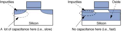
SOI also reduces soft errors due to cosmic rays and radioactive materials. In fact, the leading use of SOI has been in military and aerospace applications where radiation hardness and RF performance are critical. High costs and poor wafer quality have slowed mainstream acceptance.
A usable SOI wafer must have a consistent layer of device quality silicon—the specifications for which become more demanding at smaller design rules—on top of a high purity oxide of uniform thickness. The three most common ways to achieve this goal are separation by implantation of oxygen (Simox), bonding, and hydrogen-delamination- induced splitting (see sidebar). In Simox, the process used by IBM, a high energy oxygen implant creates an oxygen layer underneath the silicon surface. Annealing restores the surface crystal structure and allows the implanted oxygen to react with the surrounding silicon to form SiO2.
According to Ghavam Shahidi, IBM's SOI program manager, the high implant dose required by this approach damages the device surface and can drive metallic contamination from the implanter into the wafer. The high circuit densities used by modern microprocessors cannot tolerate these levels of damage or contamination. IBM manufacturers its own SOI wafers from prime silicon, maintaining tight process control and screening each lot before releasing it to production. Without these precautions, Shahidi said, inconsistent wafer quality cuts yield in half.
Yield is critical because of SOI's other limitation: cost. Because of the high oxygen concentration required, each implant tool produces only 20 wafers/day. Delivering the 20,000 wafers/month consumed by a typical fab requires substantial capital investment. SOI currently adds a hefty 10% to the finished wafer cost, before testing and packaging. Though Shahidi told Semiconductor Online the performance benefits of SOI justify the cost, he emphasized that efforts to improve productivity are underway. IBM is working on a low-oxygen, high-throughput process, which Shahidi expects to cut wafer costs in half by this time next year.
Eventually, IBM expects SOI to replace bulk CMOS as the most commonly used substrate for mainstream microprocessors and wireless electronic devices. The first products will appear in the first half of 1999, Shahidi said. The process will initially target the ASIC and RISC markets.
By Katherine Derbyshire
The Simox approach to SOI chosen by IBM allows precise control of the thickness and position of the insulating oxide layer, but at the expense of high surface damage and contamination risks. Two alternative processes address these issues.
Bonded SOI wafers avoid implantation altogether. Instead, an oxidized wafer (A) is diffusion-bonded to an unoxidized wafer (B). The backside of wafer A is polished and etched to the desired device layer thickness. In this approach, the device layer is bulk-quality silicon, free from the implant damage inherent in the Simox approach. Substantial silicon is wasted, however, and achieving a consistent layer thickness and oxide depth is difficult.
A third approach, hydrogen-delamination-induced splitting, takes advantage of both bonding and implantation. This process, developed by Soitec (Grenoble, France) under the tradename Unibond, implants hydrogen into an oxidized wafer, defining the eventual top silicon layer thickness.
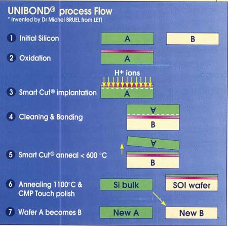
A "handle" wafer is bonded to the oxide layer. After annealing, the original wafer splits at the hydrogen layer, leaving the desired oxide thickness behind and maintaining the quality of the original crystal.
According to Andrew Wittkower, president of Soitec USA (Peabody, MA), the Unibond process delivers seven times the throughput of the Simox process at comparable cost. Quality of the two processes is comparable, Wittkower said, with both processes having advantages and disadvantages. Though Soitec orginally supplied Simox wafers, the company relies on the Unibond process exclusively for 8 in. and larger diameters.