
Slice, Rotate, and Visualize Acoustically: A New Nondestructive Tool For Inspecting IC Packages

Because it images and analyzes internal features nondestructively, acoustic micro imaging has been used for years to inspect semiconductor packages. Acoustic techniques specifically developed for IC packages have proliferated - the new 230 MHz transducer family, designed expressly to image flip chips, is an example.
The latest development lets users nondestructively image an IC package, and then manipulate the output in a variety of useful ways. For instance, with a plastic quad flat package (PQFP), the tool can make a series of 2 to 100 planar images, each focused slightly deeper within the package. Then, the user has several choices:
- Flip through the images in sequence downward from the top surface of the package. "Paging" through the images gives a good idea of landmarks on the way (the die face, for example, or the die attach) to the internal feature or defect of interest.
- The 2 to 100 images are stacked up, resembling a rectangular solid. The software can show the outside of the solid. It can rotate the solid in x, y, and z axes. It can slice through the solid at any point and at any angle to create an acoustic cross-section of the IC package.
- Instead of slicing through the solid, the software can define and remove a smaller rectangular solid to provide an image sliced along three axes of the user's choosing.
- All of the images in thumbnail size can be shown in a single display. This method presents the entire volume of the IC package at a glance.
"In this case we wanted a new tool which required little training or experience and which would give the user the ability to obtain a full acoustic view of the IC package. The imaging flexibility of this new technology makes it very easy to get the whole picture quickly."
The usefulness of acoustic micro imaging systems is based partly on the fact that they use ultrasound - mechanical energy - rather than some portion of the electromagnetic spectrum. X-ray and acoustic microimaging, for example, are largely complementary to each other. X-ray images are based on atomic mass, while ultrasound images are based on acoustic impedance and bond integrity.
In a reflection-mode acoustic microscope such as C-SAM, the ultrasonic transducer scans over the area of the IC package, switching between its transmit and receive modes hundreds or thousands of times per second. Ultrasound transmitted into the top of the IC package travels at about 3,000 meters per second, but varies in speed and impedance in the different materials of the package.
When the ultrasound meets an interface (molding compound to die face, for example), some of the sound waves are reflected back to the transducer and captured during the receive mode. There are both positive and negative echoes, depending on the upward or downward change in acoustic impedance across the interface. If ultrasound strikes a gap-type defect (a delamination, disbond, void, crack, etc.), all of the ultrasound is reflected.
In normal work, whether in the laboratory or on the production floor, the transducer's ultrasound is gated electronically. Gating accepts echoes from a level of interest (the die face, for example, if die face delaminations are the concern) and ignores echoes from other levels. The ultrasonic focus is also optimized for the level of interest. Zip-Slice, in contrast, accepts echoes from all levels of the IC package in order to construct its volumetric image.
When creating a volumetric image, the user first selects the part type in the system's software library. This step tells the system's auto-focus software how to find and characterize the IC package. The system automatically locates the part in the field of view, measures its size, and establishes the acoustic location of the upper and lower surfaces. Since the ultrasonic transducer needs access to only one side of the IC package, even board-mounted packages can be imaged.
Next the user supplies the number of horizontal slices desired (2 to 100), and selects the desired resolution. With this data, the software stores gate positions and other parameters in an AutoScan library.
Zip-Slice next scans the package once for each slice. Since each scan takes only a few seconds, the entire process takes only a few minutes. The individual scans set the gating and optimize both resolution and focus for each "slice." Producing the multiple-depth images without changing the focus appropriately, would blur and corrupt the data.
When scanning is completed, the collected data is automatically sent to the system's volumetric rendering software (Virtual Volumetric Viewing, or 3V). The first image which appears on-screen is the volumetric cube image of the IC package, showing the stacked slices. From this point users can rotate and slice the image, "page" through the individual slices, or display all of the slices simultaneously in thumbnail size.
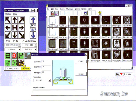
The Zip Slice menu lets the operator select the number of slices and the resolution. Thumbnails behind the menu show each of the images (32 in this case) from which volumetric rendering assembles the Zip Slice image.
Popcorn cracks are a good example of an internal defect which is usefully imaged by the technology. These cracks affect a variety of IC packages, and generally occur when excess moisture in the molding compound expands during the thermal shock of solder reflow. Popcorn cracks often curve upward in various directions from the point of origin. Often they propagate in the molding compound but do not reach the surface of the package. By slicing nondestructively downward through the package, the new technology can catch the uppermost part of the popcorn crack first, and follow the internal structure of the crack.
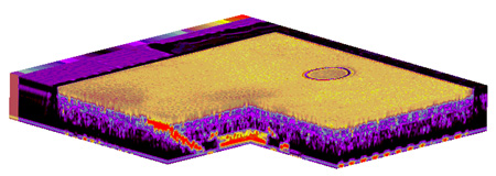
Zip Slice view of a plastic leaded chip carrier (PLCC) with a popcorn crack.
Analysis begins with a stack of 32 images. An operator-defined section was then cut through one corner of the image stack to bisect the popcorn crack. The crack begins below the die (horizontal red area in corner of cut-out). To the right of the die, a small part of the crack extends upward. To the left, the crack extends upward and reaches the surface of the package.
Image 0 (the first of the 32 images in the stack) is yellow. The circular area on the surface is a mold mark. At the left rear edge of the stack is the color map used to make the images. The area between the color map and the package is empty. Note the sectioned lead frame at the lower right of the stack.
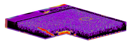
This view of the same PLCC begins with Image 4. Images 0 through 3 have been ignored, so the yellow surface image is no longer present. Note the persistence of the mold mark in the molding compound. The ability to make a corner cut-out (or vertical slice) and ignore sequences of images gives great flexibility in displaying the desired internal features.
Or - and this is where the versatility of the technology pays off - users can slice the original cube image from many points and many angles to see the popcorn crack in different ways. The thumbnail images show the entire structure of the crack at a glance.
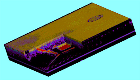
Selecting appropriate x, y, and z dimensions displays the floor of the cut-out. The red area in the corner of the cut-out is the die attach, which has been disbonded by the complex popcorn crack. To the left of the die, the popcorn crack reaches the package surface and extends horizontally along it (dark line). The black feature to the left of the surface crack is a pin locator at the top of the package. Note the lead frame details on the floor of the cut-out.
"When you are imaging and characterizing an internal defect in an IC package, it is useful to have the best understanding possible of the structure of that defect," notes Michael Oravecz, director of research at Sonoscan and one of the key developers of Zip-Slice and 3V. "This new technology gives the user an unparalleled visual sense of the internal defect, and it delivers this visual sense nondestructively. When you are trying to understand an internal defect in order to prevent its recurrence, having a fine visual feel for the defect is awfully important."
By Tom Adams
Tom Adams is a writer and photomicrographer who has written widely on semiconductor subjects. He is based in Lawrenceville, NJ.
For more information: Sonoscan, Inc., 530 East Green Street, Bensenville IL 60106. Tel: 630-766-7088; Fax: 630-766-4603.