
SIRD
Source: Tepla Inc.
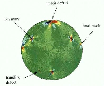
Scanning InfraRed Depolarization
The Power of Laser
Depolarization Map ![]()
The scanning infrared depolarization measurement represents an indispensable method for quality management and yield improvement in semiconductor technology. The in-line capable technique measuring on product wafers covers tasks in:
- Process control
- Process tool control
- Defect monitoring and screening
- Quality management
- Defect screening and wafer sorting in early stages of wafer manufacturing
- Slipline control in case of rapid thermal annealing procedures
- Monitoring of temperature gradients by induced stress evaluation
- Monitoring of technological procedures during wafer design
- Fracture prevention
- Final quality testing
- Input control and sorting
- Slipline control for high temperature processes
- Fracture prevention
- Control of process induced stress mainly in RTP, ion implantation, diffusion and epitaxy
- Trouble shooting
Tepla Inc. , 1321 Valwood Parkway, Suite 400, Carrollton, TX 75006. Tel: 972-247-0053; Fax: 972-247-0405.