
Rohm And Haas Purchases SUSS Coating Cluster For Resist And Spin-On Dielectric Qualification

Thick resists and photodielectrics are enabling technologies for volume production in wafer level packaging, 3D Integration and MEMS, representing some of the main markets for both companies. The system is scheduled for installation in late 2007 at Rohm and Haas' photoresist manufacturing site in Nigata, Japan.
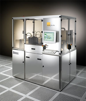
"Bringing leading edge technology like InterVia photoresists and photodielectrics to market requires our development labs to work with next generation processing equipment," says Mike Toben, Global R&D Director for Rohm and Haas Electronic Materials, Packaging and Finishing Technologies "Our goal in selecting a new coating cluster was finding a system with the combination of high throughput and state-of-the-art control, and we believe we have found that with the new Gamma XPress. The SUSS MicroTec tool will significantly enhance our R&D and customer modeling capabilities."
"We are honored that Rohm and Haas, one of the leading photoresist manufacturers, has decided to qualify its innovative resist solutions on a coat/develop system from SUSS MicroTec," comments Rolf Wolf, managing director for SUSS Micro Tec's lithography division. "With the Gamma XPress SUSS MicroTec has developed a new advanced coating cluster that combines efficient processing with flexible production setup, helping our customer to minimize the cost of ownership for the tool."
For information about Rohm and Haas Electronic Materials can be found at www.rohmhaas.com.
SOURCE: SUSS MicroTec