
Monitoring Metal Films Near the Wafer Edge

The via formation process deposits CVD (chemical vapor deposition) tungsten (W) to within 1-3 mm of a wafer's edge. Metal deposited on the beveled wafer edge can break off during chemical mechanical polishing (CMP), forming damaging particles. Therefore, any metal layer subjected to CMP must avoid deposition close to the wafer edge. Monitoring the deposition requires a metrology tool that can detect where the film ends in relation to the edge of the wafer and whether or not the deposited film is centered on the wafer. Copper processes must control the edge profile of three or more films (barrier, seed and fill layers), making the need for edge profile measurement capability even greater. The film's RMS roughness is also important as a measure of film quality and grain size.
Background
Masks and inert gas flows directed from behind the wafer are typically used to prevent edge deposition. Qualifying these deposition processes is challenging because conventional metal film measurement techniques do not have adequate spatial resolution (which must be below 100 mm) to measure closer than a few mm to the wafer's edge. Picosecond ultrasonic laser sonar (Pulse), a new technology used in the MetaPulse system[1], allows measurements in a site size less than 10 µm wide. This site size requires high-precision system automation: the system offers better than 20-µm blind radial drive precision.
Method
We used a MetaPulse system to measure thickness and roughness from the center to the edge for three 200-mm wafers with 4500 Å of W on CVD TiN. We also measured thickness and roughness along a radius less than 1 mm from the edge on a wafer with 1100 Å of PVD copper.
Results
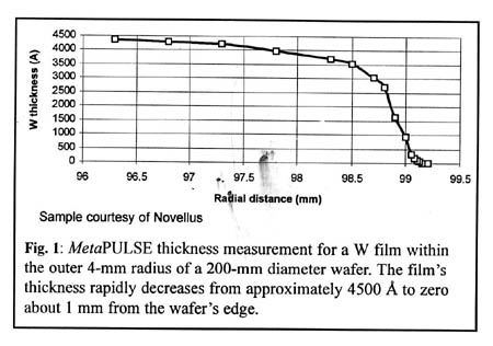
On the first W wafer, the film thickness decreased from 4500 Å to zero within the outer 4 mm of the wafer edge (Fig. 1). Thickness decreased from 3500 Å to zero between 98.5 and 99.5 mm. Near the center of the wafer, the roughness was 350 Å RMS within the measurement spot.
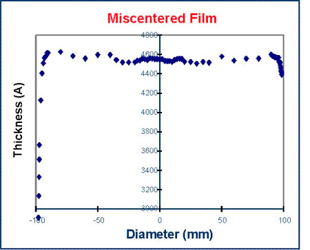
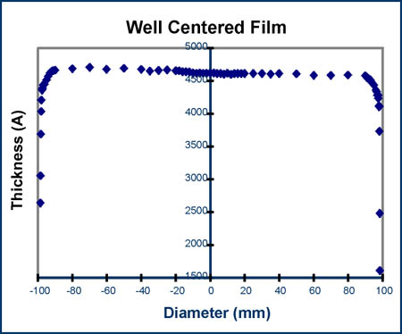
A comparison of two W/TiN wafers demonstrated that the W on the wafer in Fig. 2a was miscentered while the W on the wafer in Fig. 2b was well-centered.
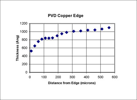
Measurements on the PVD copper film (Fig. 3), taken to qualify a new Cu process, showed that Cu deposition was not prevented at the wafer edge. This copper edge profile could lead to particle generation during polishing.
Conclusion
High spatial resolution provided by the sub 10-µm measurement spot size allows the MetaPulse system to measure in unpatterned regions less than 20 mm in diameter on product wafers. The tool can monitor not only CVD processes (where the edge is an important consideration) but also CMP processes, where polish rate may be strongly influenced by topography.
The system can determine roughness simultaneously with thickness, possibly eliminating conventional reflectivity measurements of roughness.
References
[1] C.J. Morath, G.J. Collins, R.G. Wolf, R.J. Stoner, "Ultrasonic multilayer metal film metrology." Solid State Technology, June 1997, 85-92.
Application Note courtesy of Rudolph Technologies, Inc.
For more information: Rudolph Technologies, One Rudolph Road, PO Box 1000, Flanders, NJ 07836. Tel: 973-691-1300; fax: 973-691-5480.