
IMEC Demonstrates Feasibility Of 3D-Stacked IC Integration

San Francisco, CA - At the recently concluded IEEE International Electron Devices Meeting, IMEC showed the potential of 3D integration using standard front-end techniques for via fabrication. Extremely thinned bulk-silicon die containing through silicon vias are stacked and interconnected by direct Cu-to-Cu thermo-compression bonding.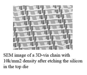
Functional through-silicon 3D-via chains were realized with densities up to 10k/mm2 and a via pitch of 10µm for a via diameter of 5µm and a via height of less than 20µm. By using Cu to fill the 3D vias and direct Cu-to-Cu bonding to interconnect the die, the resistance of the vias is consistent with bulk-Cu resistivity, without a significant contact resistance at the bonded interface.
Within the 3D-stacked IC process, the Cu vias are processed immediately after the contact layer and before processing the back-end-of-line (BEOL) metal layers using regular single damascene techniques. Subsequently, vias are opened at the wafer backside by aggressively thinning the silicon wafer down to 10-20µm using a grinding – chemical mechanical polishing – etch sequence. The thinned wafer is diced using a regular blade dicing process and after that, dies are attached and electrically interconnected to a Cu/dielectric landing substrate using a direct Cu-to-Cu thermo-compression bonding. The process is inherently extendible to wafer-scale stacking.
The 3D-stacked IC approach has several advantages compared to other advanced 3D approaches. It achieves much higher via densities than integration schemes using packaging-type technologies where wide vias are made after completion of the back-end-of-line (BEOL) layers and without requiring the use of SOI substrates. The Cu vias are processed before applying BEOL metallization leaving BEOL routing capabilities unaffected. The direct Cu-to-Cu bond avoids intermetallics formation at the bonded interface. The possibility of parallel processing of the wafers to be stacked enables compound yield optimization.
These results were obtained within IMEC's core program on (sub-)32nm CMOS, which joins forces from nine of the world's leading IC manufacturers or foundries (Infineon, Intel, Micron, NXP, Panasonic, Samsung, STMicroelectronics, Texas Instruments and TSMC).
SOURCE: IMEC