
Flash Memory Characterization, Part I
Flash memory technology allows rapid product customization and facilitates the storage of set up and diagnostic information. Because of this, product designers are looking for ways to embed flash memory in a wide range of applications. This has caused a rapid expansion in the number of production lines that now process flash memory devices. Flash memory lends itself to standard CMOS processing with minor changes. However, flash technology introduces several new material sensitivities that are not generally an issue for standard CMOS processes. Even though flash can be implemented with standard materials and familiar processing techniques, it requires new characterization methods. This article, part I includes an overview of flash memory technology and discusses leakage and defect density measurements. Part II reviews test methods for charge retention, process-induced damage, and program/erase cycling.
Contents
Flash Memory Structure and Operation
Simple Capacitor Test Structure
Triple Cell
Defect Density Measurements
References
About the Author
Flash devices are programmed and erased in a high electric field where the oxide experiences tunneling currents not found in a standard CMOS process. These high fields and currents introduce a sensitivity to various charge trapping parameters of the tunnel dielectric. The technology is subject to charge loss issues, program/disturb charge modifications, and unique process-induced charging problems. The floating gate techniques used in flash memory devices also introduce an increased susceptibility to such well-known failure mechanisms as mobile ions.
The techniques discussed below for characterization of flash memory devices can help product development and process engineers determine if design is likely to hit its yield target. More importantly, these tests and measurements can help keep an embedded flash process under control, producing high yields and reliable products.
Flash Memory Structure and Operation
A flash cell stores charge on an electrically insulated (floating) node, typically an isolated piece of polysilicon surrounded by dielectric material, that can act as a gate for a transistor. Charge is transferred onto or off of the floating node by injecting electrons through a thin "tunnel" dielectric using a high electric field applied between a "control gate" and the substrate. The control gate is generally another layer of polysilicon applied over the floating node. In some cases, a high drain voltage generates high energy electrons, allowing tunneling of electrons onto the floating node while reducing the necessary field strength across the tunnel oxide.
The charge accumulated on the floating node generates a voltage, which turns the associated transistor either "on" or "off". In his tutorial presented at the 1998 ICMTS conference, Hiroaki Hazama [1] of Toshiba Corporation showed that the typical number of electrons stored on a floating node with an area of 0.25 square microns is about 13,500. With this small number, the loss of only one electron per day would result in the loss of 27% of the total charge in 10 years. Cell leakage is an important measurement for this technology.
Charge loss can be thermally activated or activated by high fields during the programming or erasing of other cells on the same row or column. Ions in the dielectric material can migrate toward or away from the charged floating node due to the induced electric field, thus reducing or increasing the apparent charge on the node. The charge initially stored or removed from the cell during a program or erase cycle can vary due to changes in the tunneling characteristics of the cell dielectric. This variability will reduce the amount of leakage required to change the state of the cell, resulting in the same type of failure as would be caused by a high leakage rate. Each of these mechanisms should be carefully measured and monitored using specific test structures and methods.
Simple Capacitor Test Structure
The simplest test structure for monitoring a flash process is a tunnel capacitor. If the process allows metal contact to the polysilicon (poly1) used for the floating gate, then a simple capacitor can be formed between poly1 and the substrate over the tunnel dielectric. This capacitor should be at least 10,000 square microns in area. If defect density measurements are required, then a range of capacitor sizes will be needed, some much larger than 10,000 square microns. Generally, the test structure should include at least one capacitor with an area equal to the cumulative area of the flash array.
Dielectric failure is often a random but area-dependent problem due to mechanisms such as particles, metal ion contamination or damage to the silicon. However, there are also mechanisms related to the perimeter of the dielectric. A second test capacitor should usually be designed with a similar area, but a different perimeter configuration. Depending on the construction of the flash cell, more than one type of perimeter may be important. Some processes have failures associated with the corners formed in the dielectric. Thus a third type of capacitor structure may be required with the same area and perimeter dimensions but a different number of corners.
Triple Cell
Flash cells are programmed by forcing current in one direction through the dielectric and erased by forcing current in the opposite direction. The amount of charge transferred through the dielectric can be measured by the change in the cell's threshold voltage, Vt. Damage to the tunnel oxide may reduce the rate at which charge is forced onto or off of the floating gate during a program or erase cycle. Charge trapped in the tunnel oxide can change the apparent charge measured on the floating gate by an I/V characterization of the cell transistor.
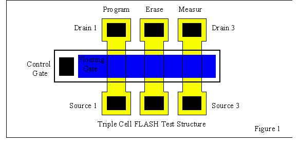
In a normal flash cell, it is difficult to determine what causes a change in the apparent value of the charge stored on the floating node. The change could be due to (a) differences in the rate at which charge is transferred across the dielectric, or (b) trapped charge in the dielectric. A test structure proposed by Yamada et. al. [2] uses three cells with a common floating gate and a common control gate (Figure 1). This structure allows programming of the cell through one transistor, erasing the cell with a second transistor, and measurement of the charge on the cell at any point in this cycle with a third transistor. The difference in the I/V characteristics of the three cells allows the measurement of the charge trapped in the gate/tunnel oxide dielectric material due to either programming or erasing.
Defect Density Measurements
Like all thin dielectrics, flash memory tunnel dielectrics must be described with a "defect density" term. Defects cause the performance of a small percentage of flash cells to be significantly different from the performance of the intrinsic or "defect free" cells. Manabe, et. al. [3] showed that this "defect density" was not a result of shorted dielectrics alone, but was also due to cells with slightly higher leakage.
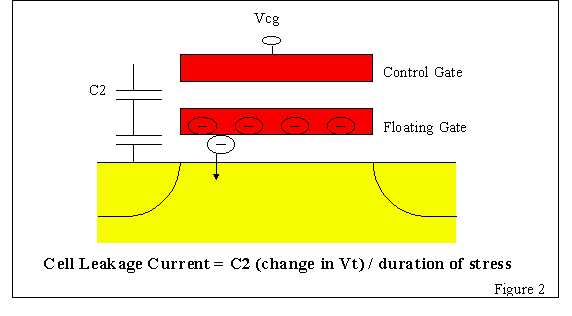
Manabe, et. al. forced a known charge onto 16 million individual gates in a large array, then measured the change in cell Vt as a function of time using a technique described by Yamada, et. al. [4]. The change in Vt could be related to the change in charge stored on the gate. The change in charge as a function of time could be used to measure the cell leakage as a function of time and stress level. Leakage currents on the order of 1x10-20 amps can be measured in this way, using:
Ileak = dQ/dt = C2 (Vt – Vt1)/t (1)
where C2 is the capacitance between the floating gate and the control gate, Vt is the cell threshold voltage after stressing at some voltage and temperature for time t, and Vt1 is the initial cell threshold voltage after charge has been stored on the cell.
For example: A flash cell has a capacitance value of 10aF between the floating gate and control gate (Figure 2). After charge is stored on the cell, the cell's Vt is measured and found to be 3.00 V. After the cell is stressed for 1000 seconds at 70°C with a voltage of –2.00 V on the control gate, its Vt is again measured and found to be 2.00 V. Equation 1 then gives the average leakage current over this stress as –1x10-20 A.
If a large array of cells is tested in this way, certain cells may exhibit anomalous high leakage currents. These cells can be considered "defects" and a defect density calculated as a percentage of cells, or as a function of thin dielectric area. The cells can also be further stressed using either a Fowler-Nordheim stress regimen or by program/erase cycling, then programmed and aged as described above. The change in leakage current as a function of the number of program/erase cycles or the amount of charge forced through the thin dielectric indicates the "reliability defect density". Manabe, et. al. showed that as many as 1% of the cells stressed in this way would show anomalous high leakage currents, thought to be due to trap-assisted tunneling.
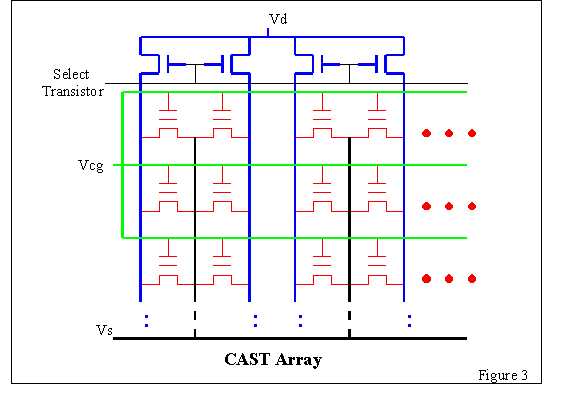
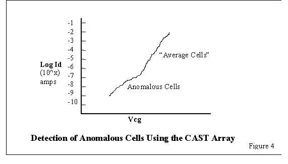
To measure a defect density, it is necessary to measure the change in Vt of a large number of cells. Large arrays of flash cells with individual row and column addressing can be used for this test. Hoffstetter and Manley [5] as well as Fan, et. al. [6] have suggested the "Cell Array Stress Test" (CAST) structure as an alternative design that provides much of the same information in a smaller area with a simpler test sequence. This structure consists of a large array of flash cells connected in parallel (Figure 3). This arrangement does not allow the measurement of individual cells but will allow characterization of the "average cell", generating a relative estimate of the number of anomalous cells (tail bits). A plot of the log of the drain current as a function of the applied control gate voltage will show the "average cell" performance at higher currents while showing anomalous cell performance at the low current end (Figure 4). The design of the CAST structure allows rapid program/erase or tunnel current stressing of these arrays so that the degradation of the anomalous and average bits can be studied from a reliability perspective.
Part II of this article will continue the discussion of flash memory characterization, focusing on charge retention, process-induced damage, and program/erase cycling.
References
1. Hazama, H., "Application of Test Structures in Flash Memories", Tutorial Short Course from the 1998 ICMTS conference.
2. Yamada, S. et. al. Proceedings of the 1993 IEDM conference.
3. Manabe, Y. et. al. "Detailed Observation of Small Leak Current in flash Memories with Thin Tunnel Oxides", Proc. IEEE Int. Conference on Microelectronic Test Structures, Vol. 11, March 1998, pp. 95-99.
4. Yamada, S. et. al. "Non-uniform Current Flow through Thin Oxide after Fowler Nordheim Current Stress", Proc. IEEE Int. Reliability Physics Symposium, 1996, pp. 108-112.
5. Hoffstetter, D. and Manley, M., "A System Test Methodology for Identifying Defect-Related Failure Mechanisms in an EEPROM Array", Proceedings of the 1994 International Conference on Microelectronic Test Structures (IEEE), vol. 7, page 114.
6. Fan, M. et. al. "New Characterization Methodology for flash Memory Cell Using CAST Structure" Proceedings of the 1998 International Conference on Microelectronic Test Structures (IEEE cat. # 98CH36157), pp. 113-117.
Timothy Turner is Director of Structures Engineering in Keithley's Semiconductor Division where he is responsible for design and development of wafer test structures and device reliability algorithms, which are part of Keithley's Wafer Level Reliability (WLR) product line. He previously owned and operated Turner Engineering, specializing in accelerated test methods that allow reduced time to market, high stable yields, and assured reliability for semiconductor fabs. His 20 years of experience in semiconductor reliability includes organizations such as the Reliability Analysis Center in Rome, NY and Mostek Corporation in Carrollton, TX. He has been issued six US patents in the field of semiconductor processing, and has published more than 25 papers in the field of semiconductor reliability and processing.
Keithley Instruments, Inc.
28775 Aurora Road
Cleveland, Ohio 44139
Phone:+1 440-248-0400
Fax: +1 440-248-6168