
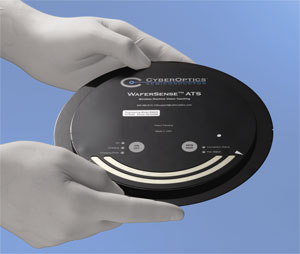
CyberOptics Semiconductor Introduces WaferSense Automatic Teaching System

Operating and maintaining modern 200 mm and 300 mm semiconductor process equipment is believed to be costly because it often requires lengthy downtime and expensive consumables. Equipment and maintenance engineers, therefore, are continually looking for opportunities to reduce downtime as well as diagnose and correct problems faster. Equipment availability and performance can be raised by teaching wafer transfer locations faster and more accurately. Today's robot "teaching" process (i.e., determining wafer transfer coordinates and loading them into the robot's controller software) requires technicians to manually direct the robot's motion and estimate wafer transfer positions. This process is believed to be not only labor intensive, but inaccurate because coordinates for most teach positions are "eyeballed" and subjective. The current labor-intensive and inaccurate procedures also require that equipment be taken off the production line and partially dismantled during maintenance.
CyberOptics claims that WaferSense ATS is an innovative measurement technology that provides accurate wafer transfer coordinates for robotic handling while reducing equipment downtime and wafer scrap. Wireless and wafer-like, the ATS can be handled like a wafer. Once inside semiconductor equipment, using machine vision technology, it "sees" targets that mark wafer transfer locations, such as load locks and process chambers, and transmits their digital coordinates to the user. Because there is no need to dismantle the equipment or cool it below maintenance temperatures, fabs can save qualification time and consumables. The ATS relays live video and real-time coordinate data via graphical user interface making equipment checks and adjustments fast and easy. The live video allows engineers to look for lost or broken wafers without opening the tool.
WaferSense ATS is available for 200 mm and 300 mm equipment and is accurate to +0.1 mm (x and y positions) and +0.5 mm (z position). Easy-to-use software logs data for later comparison and analysis to detect errors in wafer handling, and helps the user "train" the ATS to recognize new types of targets. Hard data and repeatable coordinates eliminate technician-to-technician variations in calibration technique to eliminate wafer scrap due to mishandling and eventually increase yield.
"As wafer geometries shrink and fab automation grows, it becomes critically important to teach accurate and repeatable wafer transfer positions to achieve maximum productivity and yield," said Craig Ramsey, General Manager of CyberOptics Semiconductor. "WaferSense ATS provides coordinate data to maintenance engineers so that robot transfer coordinate teaching is fast, accurate, and reproducible. With our ATS, fabs can significantly reduce downtime and scrap."
WaferSense ATS Key Specifications
- 200 mm or 300 mm wafer-like form factor
- Accurate to ¡¾0.1mm (¡¾0.004") x and y position; ¡¾0.5mm (¡¾0.02") z position
- Packaging - low outgas carbon fiber, polycarbonate label
- On-board camera captures live video from inside semiconductor equipment as an on-board image processor reports the xyz offset from the teaching wafer to a target present inside the equipment
- Measures offsets to targets 6.5 mm to 45 mm (0.25" to 1.8") below the teaching wafer
- Teaching wafer can withstand exposure to 120¢ªC (5 min or less) if not in direct contact with heat source
- Vacuum compatible so equipment stays sealed during troubleshooting and teaching
- TeachView software displays live video and offset measurements while optionally logging offsets and user comments.
- TeachTarget helps the user train ATS to find most circular features
- Bluetooth communications; USB-compatible link
- For use with Windows 2000, XP and Vista operating systems
The WaferSense ATS product includes teaching wafer, charging clean box, USB link and application software (TeachView and TeachTarget). The WaferSense ATS joins other WaferSense products including the Auto Leveling System (ALS) and the Auto Leveling System for Reticles (ALSR), precise wireless, wafer-like devices for accurate leveling of semiconductor wafer processing and automation equipment. For more information, you can visit www.CyberopticsSemi.com.
SOURCE: CyberOptics Semiconductor