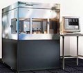
Critical Dimension Metrology

SNP's Non-Destructive Cross Sectioning (NDCS) provides an accurate profile (or set of multiple profiles) of a deep submicron feature or line without physical cross-sectioning. Linewidths, depths, sidewall slopes, and corner geometries are measured anywhere from the top to the bottom of lines, trenches, and vias – information not obtainable from CD-SEM top-down views. Non-conductive samples, such as photomasks, are handled without the problematic charging effects typical of electron-beam-based metrologies.
The tool currently addresses three metrology requirements in the semiconductor fab:
- CD-SEM Calibration— Selected features are measured by both SNP and CD-SEM for CD-SEM calibration. As a complementary technique, Stylus NanoProfilometry adds accuracy to the precision and extremely high throughput of the CD-SEM to provide quantitative fab-to-fab and tool-to-tool comparisons.
- Process Variation Detection for Lithography— SNP makes automated, non-destructive exposure/focus matrix array measurements for stepper calibration, certification, and optimization. These measurements replace physical cross-sectioning and imaging at multiple points, a time-consuming process. The non-destructive SNP method offers both CDs and CD statistics over the entire exposure area on an intact substrate quickly and with immunity to substrate charge build-up.
- 3-Dimensional Nano-scale Metrology for IC Development— Stylus NanoProfilometry supports the most advanced IC development efforts and will also be a viable primary CD metrology tool in production on future reduced linewidth generations.
In probe measurements, both tip and feature geometries contribute to the raw data obtained. The tip's contribution must be eliminated from the data to ensure accuracy. The shape of the tip on the nano- scale must not change during the measurement from wear or contamination. In the SNP tool, tips are completely characterized using on-board standards, and a library of exchangeable tips is maintained for various applications. Computer algorithms automatically calculate the true sample profile from the scan output by removing the contribution of the tip shape from the raw data.
Sample damage and tip wear are minimized because SNP's Pixel-Only Sampling ensures minimal sample contact. The tip approaches the surface under Force-Controlled Contact and Angle-Controlled Contact. One data point is obtained at each pixel (defining resolution), and the tip is fully retracted from the surface between measurements. Artifacts due to moisture or charging are eliminated.
The heart of the SNP measurement system is a compact (10mm x 5mm) and rugged Probe Assembly consisting of a silicon balance beam with an integral probe tip. The complete probe assembly is automatically exchanged as required. The Balance Beam Force Sensor consists of the probe assembly plus the base plate with capacitive sensors for detecting the force between the tip and the surface of the sample.
Surface/Interface Inc., 260 Santa Ana Ct., Sunnyvale, CA 94086-4512. Tel: 408-732-7111. Fax: 408-732-7191.
