
Controlling adhesion stack deposition
Contents
• Introduction
• Method
• Results
• Conclusion
• For more information
Introduction
For x-ray techniques such as XRF and XRR, counting times of many minutes per site are needed to obtain acceptable measurement precision for films thinner than a few hundred angstroms.
The reliability of metal film thickness measurements is generally poor for optical techniques like spectroscopic ellipsometry, because the optical properties of metals tend to depend strongly on deposition conditions and the measurement environment. Optical constants for dielectric materials tend to be much closer to the ideal.
The reliability of thicknesses inferred from electrical sheet resistance measurements also suffers from the tendency for the bulk resistivity of metals to vary from sample to sample. CVD films in particular may contain highly variable concentrations of contaminant species such as carbon. For very thin films, other factors such as the condition of the top and bottom surfaces, and the electronic mean free path can have a strong influence on the sheet resistance even when the bulk resistivity is well-known. As a result, it is generally very difficult to reliably determine the thickness of any metal film whose thickness is comparable to the electronic bulk mean free path.
The MetaPulse can routinely make metal thickness measurements for single or multi-layer films as thin as 25 Å. MetaPulse measurements of ultrathin (CVD TiN / (IMP) Ti stacks can be made on patterned wafers at high throughput and with long term 3-sigma repeatability for each film of better than 0.5A.
Back to top
Method
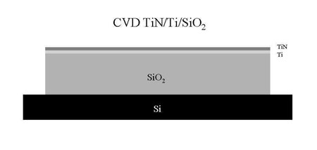
We prepared samples by depositing a thin IMP Ti film followed by a CVD TiN film on oxidized eight-in silicon wafers (Figure 1). Depositions were carried out in separate chambers connected by a common vacuum space. Following the CVD TiN deposition, the wafers were exposed briefly to a reducing plasma. MetaPulse measurements, made outside the deposition system, typically required less than 10 seconds per site.
A pulse measurement focuses an ultrafast laser pulse on a region of the film surface. Absorption of this light pulse causes a small rise in temperature (typically 5 to 10°C) of the film near the surface. A thermal stress wave propagates away from the surface at the speed of sound in that material. The small amount of heat deposited by the laser pulse is non-destructive and dissipates into the filmstack in a few nanoseconds, playing no further role in the thickness measurement.
Back to top
Results
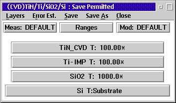
Figure 2 shows the echoes returning from a sample consisting of a 56.5 Å CVD TiN film deposited on a 108.9A IMP Ti film.MetaPulse simultaneously found the thickness of the underlying thermal oxide layer to be 758Å. The density of the CVD TiN film was 3.8 g/cm3. Figure 3 shows the MetaPulse filmstack used to analyze the sample.
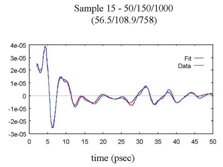
Measurements made on this sample over a period of thirty days gave a standard deviation of less than 0.35Å for both films. Measurements were made at a single site.
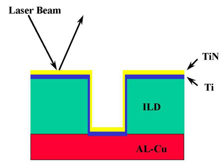
Although the measurement site size fits comfortably into a typical 50 micron square scribe-line test structure, it is generally much larger than a via or contact. Instead, measurement sites are selected in nearby planar regions of patterned wafers (Fig. 4). As the thickness of CVD TiN/Ti adhesion stacks shrinks, it is important to monitor the thickness and quality of the deposited films with precision and repeatability.
Conclusion
MetaPulse measurements of very thin (CVD) TiN / (IMP) Ti stacks have been made on films of both metals as thin as 25Å. Sub-angstrom 3-sigma repeatability results over 30 days of single-site measurements demonstrate that MetaPulse can be used as an effective monitor for this increasingly common and challenging deposition process.
Back to top
For more information
1. C.J. Morath, G.J. Collins, R.G. Wolf, R.J. Stoner, "Ultrasonic multilayer metal film metrology." Solid State Technology, June 1997, 85-92.
2. Monitoring PVD Adhesion Stacks, RTI Application Note.
3. Van de Ven, Evert, "Cost-Effective Thin Film Processes Will Prevail," Semiconductor International, January 1994, 41-42.
4. Littan, Karl et. Al. "CVD TiN for Sub-0.5 um Technology" Semiconductor International, July 1994, 183-184.
5. "Handbook of Optical Constants of Solids," edited by Edward Palik, Academic Press, New York, 1985.
Application Note courtesy of Rudolph Technologies, One Rudolph Road, PO Box 1000, Flanders, NJ 07836. Tel: 973-691-1300; Fax: 973-691-5480.
Back to top