
Applied Materials' New Etch System Overcomes Barriers To Etching High-k/Metal Gates

"This is the first etch system specifically designed to meet the challenges of HK/MG production," said Tom St. Dennis, senior vice president and general manager of Applied Materials' Silicon Systems Group. "Our customers are very enthusiastic about the new technology offered by the Carina system and we have multiple installations at leading logic and memory semiconductor manufacturers worldwide."
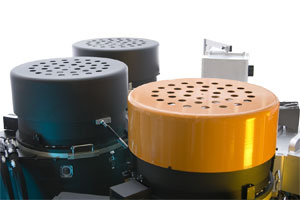
Key to the system's benchmark performance is its proprietary high temperature cathode. Processing at high temperatures produces smooth, vertical profiles without the high-k "foot" and silicon recess that plague conventional-temperature alternatives. In addition, the high temperature prevents the etched material from re-depositing on the wafer and eliminates the need for complex wet/dry process combinations to remove the residue. Advanced chamber materials deliver long-term process stability and the lowest cost-of-consumables of any available advanced gate etch system.
Applied's Carina Etch technology will be showcased at SEMICON West as part of Applied's integrated HK/MG technology: a comprehensive portfolio of fully characterized systems and processes for building HK/MG structures in high volume production.
SOURCE: Applied Materials, Inc.