
Aluminum Damascene Balances Cost, Performance

By Katherine Derbyshire
In the microprocessor world, speed is king. Each MHz of clock speed translates directly into higher selling prices. Microprocessor manufacturers seek to reduce circuit delays at all costs, which means decreasing interconnect resistance. The microprocessor performance premium is driving much of the current interest in copper metallization (See related article).
The IC industry is not a monolith, though. For many components, particularly in the rapidly growing telecommunications segment, high frequency performance is more important than computation speed. For these chips, capacitance, which affects crosstalk and dynamic power dissipation, is a more serious concern than resistance.
Meanwhile, in the DRAM world, cost is king. One memory chip is pretty much like another, forcing DRAM manufacturers to compete primarily on price. Circuit performance earns a relatively small performance premium.
These differing needs encourage different approaches to advanced metallization. Retooling for any new material is expensive, so chipmakers need to see compelling reasons to switch. If presentations at the recent IEEE Interconnect Technology Conference (IITC) are an indication, many companies do not think the benefits of copper outweigh the disadvantages.
For example, dual damascene, the copper integration scheme of choice (See related article), eliminates mask steps and replaces costly metal etch steps with much simpler oxide etch. A desire to gain the cost advantages of dual damascene without the added expense of copper has sparked substantial interest in aluminum dual damascene integration. Aluminum is more compatible with existing processes than copper, and also avoids copper's notorious contamination risks.
Improved electromigration lifetimes are often cited as another advantage of copper. Yet, as L. A. Clevenger, of the IBM/Siemens DRAM Development Alliance (Hopewell Junction, NY) and coworkers reported at IITC, CVD/PVD Al structures have dramatically better electromigration resistance than etched aluminum. K. Kikuta and coworkers at NEC Corporation (Sagamihara, Japan) reported a 4x improvement in electromigration lifetimes for dual damascene aluminum relative to conventional tungsten plug metallization. With this improvement, Clevenger expects dual damascene Al to be viable through the 1 Gbit DRAM generation.
The IBM/Siemens group considered two possible process integration schemes. The first used a PVD Ti/Al liner, followed by PVD Al deposition, in situ reflow, and CMP planarization. The second used CVD TiN/Al liners, with CVD/PVD Al fill. After the reflow process, transmission electron micrographs showed substantial TiAl3 formation, while very little TiAl3 formed in the CVD/PVD process. Clevenger blamed this TiAl3 for higher sheet and contact resistance in the reflow films. Al reflow also had unacceptable gap fill performance below 0.225 nm, while the CVD/PVD vias maintained good yields down to 175 nm.
According to Toshiba's (Yokohama, Japan) N. Nakamura and coworkers, the standard damascene integration scheme faces two serious issues. The first is trench depth control. Since etch rate varies with trench width, some trenches will be deeper than others after the same etching period. Feature size dependence, always present, is exaggerated by the lengthy via etch. Second, etching of unlanded vias leaves narrow voids along the sidewall of the underlying line. These voids are much smaller than the minimum feature size, and very difficult to fill with metal. Addition of a SiN etch stop prevents both problems, improving trench depth uniformity to 1.1% versus only 3.2% without the stop layer in the Toshiba study. However, Nakamura explained, SiN has a high dielectric constant (k=7). Placing etch stops directly above and below the metal lines, where corner effects concentrate charge, leads to a 13% increase in capacitance. Since first generation low-k dielectrics are only expected to provide an 11% capacitance reduction (See related article), SiN etch stops threaten to absorb the low-k benefit.
To solve the problem, Nakamura suggests an alternative integration scheme, placing the etch stop above a 50 nm separation layer. According to model calculations, the separation reduces the capacitance increase from the SiN layer to 6%. Removing the separation layer requires a small overetch after breaking through the SiN layer.
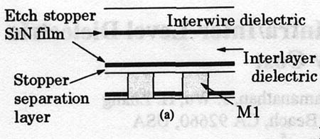
Elevated double stopper process flow.
(a) Deposit stopper separation layer, via SiN stop layer, interlayer dielectric, trench SiN stop layer, and intralevel dielectric, in sequence,
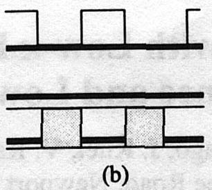
(b) etch trench holes,
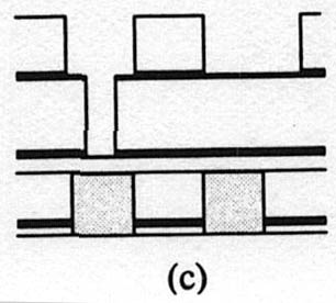
(c) etch via holes,
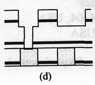
(d) breakthrough to metal in via holes, and
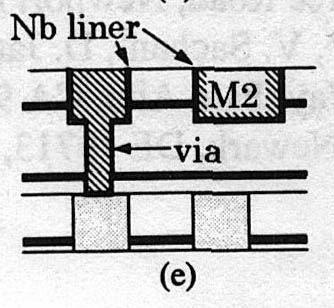
(e) deposit niobium (Nb) liner, fill with aluminum, and polish.
B. Zhao of Rockwell Semiconductor Systems (Newport Beach, CA) and coworkers integrated dual damascene Al with a silsesquioxane dielectric. An oxide cap layer protected the low-k material during photoresist strip and served as an etch buffer layer. The group measured a 30% (k=2.3) interlevel capacitance reduction and a 20% reduction (k=2.7) for the intralevel film, relative to etched-Al wiring with SiO2 dielectrics.
The existence of the SIA Roadmap, the prominence of Sematech (Austin, TX) and other industry consortia, and the transformation of equipment companies into process suppliers (See related article) create a somewhat misleading image of chip companies advancing technology in lockstep. These differing approaches to advanced metallization reinforce the important differences in technology requirements and business fundamentals within the IC industry.