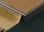
Akita Elpida Memory Successfully Develops World's Thinnest 1.4 Mm MCP With 20 Stacked Dies

Akita, Japan - Akita Elpida Memory, Inc. ("Akita Elpida"), announced the successful development of a 1.4 mm thick Multi Chip Package (MCP) with 20 stacked dies, making it the world's thinnest. 
Its operations beginning in October of last year, Akita Elpida is a new company established in July, 2006 by one of the leading global suppliers of Dynamic Random Access Memory (DRAM), Elpida Memory, Inc. ("Elpida"), with a business scope focusing on semiconductor back-end processes. Akita Elpida is currently applying its high-level technical strengths and manufacturing know-how it has developed as a member of the Hitachi, Ltd. group, as it currently focuses on developing and manufacturing cutting-edge, highly value-added packages known as MCPs and Package-on-Packages (PoPs), centering on products with 2 or 3 stacked dies.
Nowadays, as portable devices such as mobile phones and digital still cameras become even thinner and more compact as well as more highly functional, demands are being made for greater sophistication of semiconductor products such as flash memories, DRAMs, and logic which bring these features into reality. Furthermore, demand continues to rise for 5- and 7-die stacking as well as for achieving compact, thin packages.
Responding to such market needs, the development group of Akita Elpida took up the challenge to develop multi-chip stacked thin packages, thereby achieving their current success.
Akita Elpida's exceptional technical skills which lead to the development of the world's thinnest package are introduced in the following process sequence:
- Grinding technology to achieve 30 micrometer thick chips
- Handling technology for 30 micrometer thick wafers
- Technology for picking up and die-attaching 30 micrometer thick chips
- 40 micrometer low loop wire bonding technology
- Overhang wire bonding technology
- Technology for injecting resin into narrow gap
Akita Elpida, plans from now on to put this package technology to work to establish high-yield and low-cost manufacturing technology for multi-chip stacked packages such as existing 5- and 7-die multi-chip stacked packages, thereby doing their utmost to expand their business. Moreover, they plan to team up with equipment manufacturers as well as those of materials to aggressively develop state-of-the-art, highly value-added packages and related manufacturing technology as they respond to customer and market demands.
SOURCE: Elpida Memory, Inc.
