Ultra-Thin Diselenides Could Supplant Silicon In Next-Generation Electronics
By Jof Enriquez,
Follow me on Twitter @jofenriq

Layered two-dimensional materials that are as efficient, but thinner than, silicon semiconductors, could power future electronic circuits and devices, according to Stanford researchers.
Since the 1960s, silicon has been the standard base material for integrated circuits that power most electronic devices and equipment. Silicon has the ability to "rust" to insulate circuitry, a characteristic that most other semiconductor materials lack. Two-dimensional semiconductors and exotic materials, such as gallium nitride (GaN), are currently being tested as alternatives to silicon.
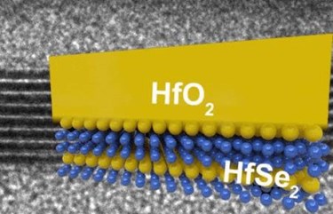
Recently, scientists at Stanford University found that two layered 2D semiconductors – hafnium diselenide and zirconium diselenide – have the ability to "rust" even better than silicon by forming so-called “high-K” insulators that make circuits more efficient.
“It’s a bit like rust, but a very desirable rust,” said Eric Pop, an associate professor of electrical engineering.
When they shrunk the diselenides to subnanometer-thin single layers, Pop and colleagues realized that the ultrathin semiconductors exhibit another one of silicon's desirable traits, which is a moderate band gap (1.1-eV) that allows low-voltage operation with minimal leakage current.
During testing, the 2D materials maintained a band gap in the 0.9- to 1.2-eV range, right in the sweet spot that "allow[s] low-voltage operation of future electronics but [is] large enough to enable >106 on/off current ratios, along with the benefits of 2D materials (namely, an atomically thin body for ultrascaled transistors)," the Stanford scientists wrote in the Aug. 11 issue of Science Advances.
It's the first time two key attributes of silicon for large-scale technological integration in a 2D nanomaterial was demonstrated.
In addition, the Stanford team said they were able to fabricate an ultra-thin layer of diselenides just three atoms thick, or about two-thirds of a nanometer.
“Engineers have been unable to make silicon transistors thinner than about five nanometers, before the material properties begin to change in undesirable ways,” Pop said.
The groundbreaking atomic scaling makes it possible to build transistors up to ten times smaller than current silicon-based ones with the same (if not better) efficiency. The performance of future transistors consisting of these new materials will rely on further improvements with refined processing, electrical contacts, and interfaces.
“Silicon won’t go away,” said Pop. “But for consumers this could mean much longer battery life and much more complex functionality if these semiconductors can be integrated with silicon.”
