
OptoSigma's Linear X-Y Stages Integrated Into Hi-Res Thin Film Stress Mapping System

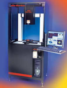 Santa Ana, CA — OptoSigma Corporation, a premier opto-mechanical, optics, and optical coatings supplier for OEM applications announces the integration of their Linear X-Y stages into a new flexible, high-resolution scanning curvature and stress measurement system from k-Space Associates, Inc. The kSA MOS Ultra-Scan is a fully integrated, ex-situ tool capable of mapping the induced thin film stress on semiconductor wafers, optical mirrors, lenses, or nearly any highly polished surface, with unprecedented accuracy. OptoSigma's X-Y stages were integrated into this unit by k-Space Associates to provide flexibility and accuracy in this novel 2-D laser system that currently offers up to 200mm x,y scanning range with 2 micron resolution.
According to k-Space Associates Sales and Marketing Director, Eric Friedman, "OptoSigma has a very good price/performance advantage over their competition because of their broad product line for OEM applications. We have been extremely happy with their X-Y stages for this application, and the availability of higher resolution stages makes for an easy decision toward integration into our next-generation systems."
"The kSA MOS Ultra-Scan offers 10x higher stress resolution, lower noise, and more powerful mapping capabilities than any other system currently available," notes Steve McNamee, OptoSigma's Vice President of Operations. He adds, "It‘s been a pleasure to work with the talented engineers at k-Space Associates on this innovative, 2-dimensional laser array scanning system. We look forward to future projects with k-Space, providing solutions for unique challenges in this exciting market."
About OptoSigma Corporation
OptoSigma Corporation, based in Santa Ana, California, is a manufacturer and distributor of optics, optical coatings and opto-mechanical devices. Founded in 1995, OptoSigma offers unparalleled customer service while delivering high performance products such as standard and custom optical components, thin film optical coatings, manual and motorized positioners, X-Y stages, stepping motor actuators and piezo stages for a variety of applications and industries. Please visit www.optosigma.com for more details.
k-Space Associates, Inc.
k-Space Associates, Inc., Ann Arbor, MI, is a leading supplier of thin-film and wafer characterization products for use with MBE, MOCVD, PLD, PVD, sputtering and evaporation systems since 1992. Using advanced optical imaging technology, our products can detect thin-film stress, strain, tilt, wafer curvature, deposition rate, layer thickness and determine absolute semiconductor wafer temperature. By closely listening and collaborating with our worldwide customer base, we have become leaders in advanced instrumentation and software for the surface science and thin-film industries. For more information, please visit our web site at www.k-space.com.
Source: OptoSigma Corporation